- Applied Materials opens $500 million Tampines Campus, doubling Singapore cleanroom capacity
- Facility uses autonomous robots and AI-assisted quality inspection systems
- Expansion creates 1,000 jobs, supports global AI chip infrastructure demand
- Campus targets Green Mark Platinum certification with zero-water-waste systems
Applied Materials has inaugurated a $500 million manufacturing and R&D campus in Singapore, more than doubling its advanced cleanroom capacity in the city-state to meet surging global demand for AI chip production equipment. The new facility, already operating at volume production, is focused on serving chipmakers that are expanding production to meet increasing AI-driven demand. For plant managers and manufacturing engineers, this expansion signals both the semiconductor industry’s capacity constraints and the urgent need for equipment suppliers to scale advanced automation capabilities.
What Makes the Tampines Campus Different from Traditional Manufacturing Facilities?
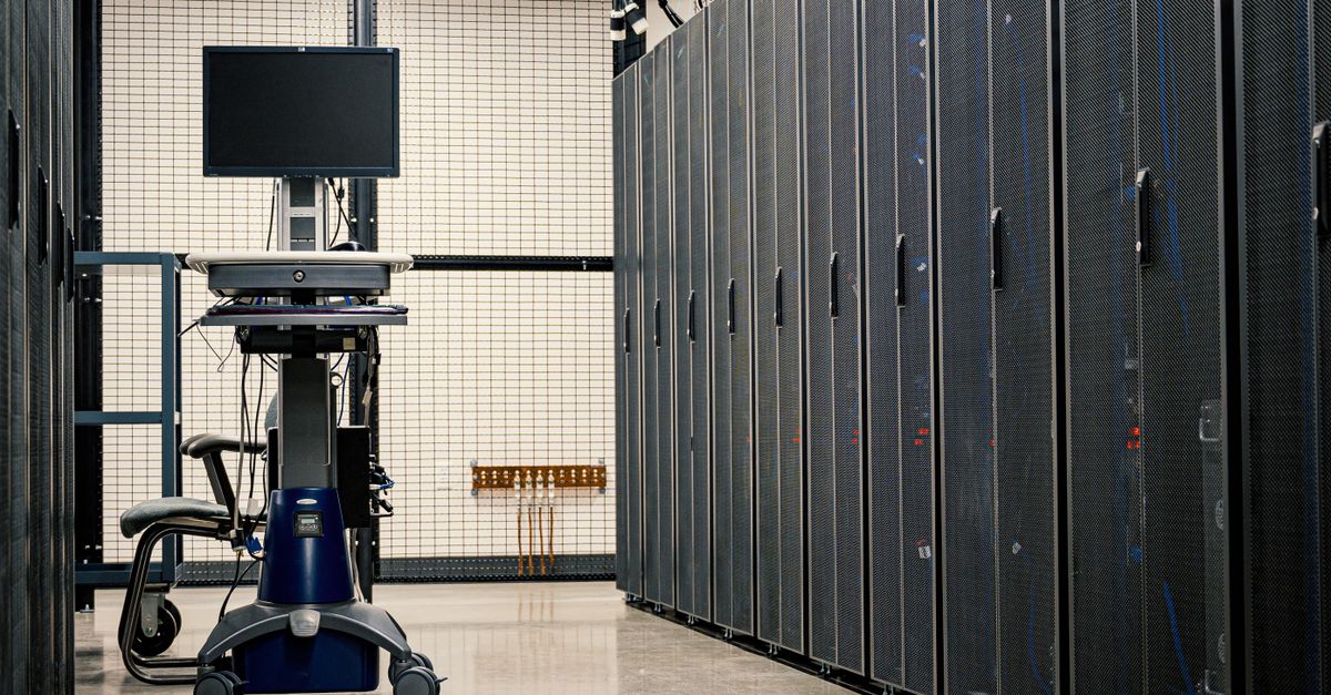
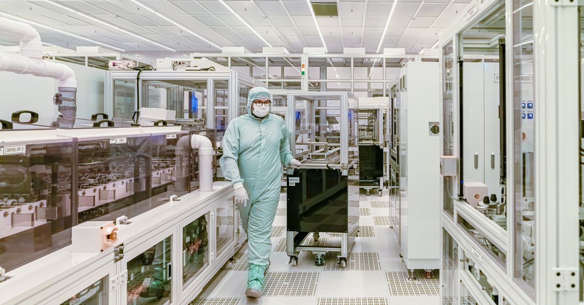
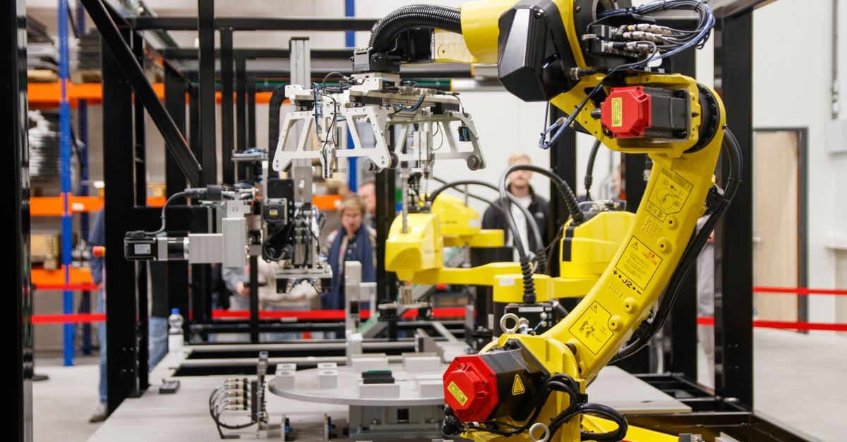
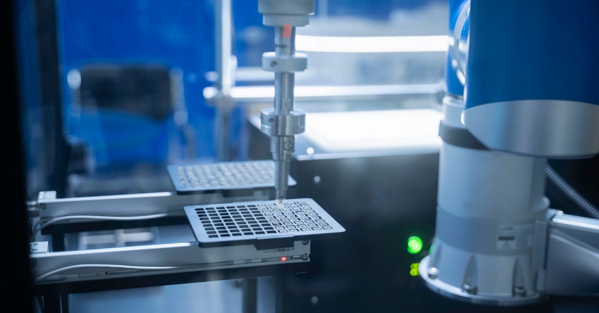
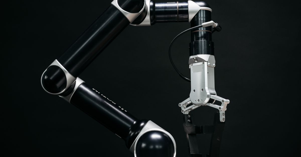
The facility deploys Autonomous Mobile Robots (AMRs), autonomous assembly and testing systems, and AI-assisted quality inspection—deepening integration between manufacturing, R&D and ecosystem partners to accelerate time-to-market for new technologies. Augmented and virtual reality (AR/VR) tools further support technician training and precision maintenance operations. This approach mirrors broader industry trends where robots enhance manufacturing workers rather than replace them, particularly in precision-driven environments like semiconductor equipment production.
Cleanroom AMRs are extensively utilized to transport wafers between process tools, clean floors and surfaces, and monitor environmental conditions. Their ability to operate continuously and autonomously ensures that wafer fabrication lines remain free from contamination and bottlenecks, thereby maximizing yield and throughput. The global semiconductor cleanroom AMR market is experiencing a compound annual growth rate of 19.6% from 2025 to 2033, demonstrating the critical role automation plays in next-generation fabs.
Designed to achieve Building and Construction Authority (BCA) Green Mark Platinum Certification, the highest tier of Singapore’s green building rating system, the campus features an onsite solar panel system, LED lighting, low-carbon concrete construction, a closed-loop water reclamation system for zero water waste, and a Smart Building Management System that monitors energy and water consumption in real time. These sustainability measures address growing pressure on semiconductor manufacturers to reduce environmental impact while scaling production.
How Does This Fit Into Global Semiconductor Supply Chain Dynamics?
Over the past several years, Applied has nearly doubled its global manufacturing capacity, including the new Tampines Campus, and the company has invested more than US$400 million in its U.S. equipment manufacturing infrastructure over the past five years. Additionally, Applied’s new US$5 billion EPIC Center in Silicon Valley, set to become operational this year, represents the largest-ever U.S. investment in advanced semiconductor equipment R&D. A traditional chip development cycle is a serial compartmentalized process, but the EPIC model and infrastructure will drastically reduce that time, enabling parallel development, agile handoffs and early access to next-generation processes across the ecosystem. This accelerates product roadmaps, increases commercial success rates and amplifies the return on R&D investments.
The strong start to 2026 reflects continued industry investment in the capacity and infrastructure needed to support AI-driven semiconductor growth. Global semiconductor equipment billings rose 14% year on year to USD $36.55 billion in the first quarter of 2026, according to SEMI. The total was a record for the industry. This investment surge is driven by unprecedented AI infrastructure buildout, with total semiconductor revenues forecast to reach $1.29 trillion in 2026, up 52.8% year over year from $842.8 billion in 2025.
The Tampines Campus marks a major milestone in Applied’s Singapore 2030 plan to strengthen the company’s global manufacturing and R&D capabilities, broaden technology ecosystem partnerships and promote local workforce development. With the expansion, Applied anticipates adding approximately 1,000 new local jobs over the next few years to support industry growth and technology commercialization. It announced separate collaborations with the National University of Singapore (NUS) and the Singapore Institute of Technology (SIT) on Wednesday, alongside the opening of its new campus in Tampines. The work links research and training to two problems in chipmaking: the long cycle of experiments needed to develop new materials and processes, and the need for engineers who can work across manufacturing, AI and automation.
What Are the Broader Industry Implications for Manufacturing Professionals?
Tightness in the chip supply chain will remain through at least the end of 2026. However, AI chip manufacturing is becoming a binding constraint on the pace of the AI compute buildout. For equipment manufacturers, this creates both opportunity and pressure: chipmakers need more capacity faster, but physical constraints—from helium shortages to power infrastructure bottlenecks—are forcing the industry to optimize existing processes rather than simply adding capacity.
The emphasis on intelligent manufacturing at the Tampines facility reflects this reality. In 2026, AI infrastructure investment is actively reshaping global semiconductor manufacturing, PCB (printed circuit board) production capacity, material availability, and long-term supply chain planning across the electronics manufacturing sector. The rapid expansion of hyperscale data centers, advanced networking platforms, GPU (graphics processing unit) computing, and AI server infrastructure continues driving demand for increasingly complex electronic hardware. Manufacturing professionals must prepare for tighter allocation of advanced materials and components, even as overall demand continues to accelerate.
Applied Materials’ dual investment strategy—expanding both Singapore manufacturing and the Silicon Valley EPIC Center—demonstrates a geographic hedging approach increasingly common among semiconductor equipment suppliers. The new US$500 million (S$600 million) Tampines Campus more than doubles Applied’s advanced cleanroom capacity in Singapore and strengthens the company’s global manufacturing footprint, which also includes facilities in the United States, Europe, Israel and Taiwan. This distributed manufacturing model mirrors strategies seen in Europe’s Chips Act initiatives, where geopolitical considerations increasingly shape manufacturing location decisions.
The Tampines Campus expansion demonstrates that advanced manufacturing for AI infrastructure requires more than capital investment—it demands integrated automation, sustainability engineering, and workforce development. Plant managers should note the emphasis on autonomous systems and AI-assisted quality control, which are becoming baseline requirements rather than differentiators. As semiconductor equipment demand continues outpacing supply through 2026, companies that can demonstrate both manufacturing scale and technology integration speed will capture disproportionate market share. The 1,000-job expansion also signals that even highly automated facilities require substantial skilled workforce investment, particularly engineers capable of bridging manufacturing execution, automation programming, and AI system integration.
Q: How do autonomous mobile robots in semiconductor cleanrooms differ from standard industrial AMRs?
Semiconductor cleanroom AMRs must meet ISO cleanroom class 3 requirements, meaning they produce minimal particle emissions and feature ESD-certified components. They operate continuously in ultra-clean environments, transporting wafers between process tools while monitoring environmental conditions to prevent contamination that could destroy yields.
Q: Why is Applied Materials investing heavily in both Singapore and Silicon Valley simultaneously?
The dual investment strategy serves different purposes: the Singapore Tampines Campus provides high-volume manufacturing capacity close to major Asian chipmakers, while the $5 billion EPIC Center in Silicon Valley focuses on collaborative R&D to accelerate technology commercialization from research to production. This geographic distribution also mitigates geopolitical supply chain risks while maintaining proximity to key customer regions.
Article Source: Applied Materials Expands Singapore Manufacturing to Support AI Chip Demand