- AI models improve defect capture rates but 70% fail after pilot phase
- Wafer edge inspection proves critical for hybrid bonding yield improvement
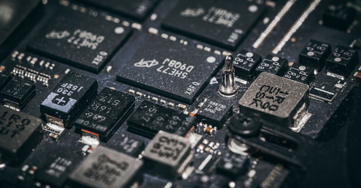
- Chiplet packaging creates massive data explosion requiring scalable analytics
- Deep learning outperforms traditional rule-based inspection algorithms significantly
Semiconductor manufacturers are deploying artificial intelligence to detect defects across hundreds of process steps, from lithography to advanced packaging. While AI models excel at distinguishing yield-killing defects from nuisance anomalies, approximately 70% of AI initiatives stall after pilot implementation, creating a critical gap between proof-of-concept success and factory-wide deployment. This scaling challenge matters because a 1% yield gain at advanced node die values pays back the entire inspection platform investment within a single production month, making defect detection one of the highest-ROI applications for AI in manufacturing.
Engineers targeting yield improvement projects face a paradox: AI models demonstrate impressive accuracy in controlled pilots but struggle when deployed across enterprise production environments. The five gaps that reliably kill scale are missing data infrastructure, absent change management, governance that was never built, metrics untethered from business outcomes, and executive sponsorship that evaporates after the demo. Traditional algorithms require tedious manual parameter adjustments when new defect types emerge, whereas AI models can adapt through training data alone.
How Do AI Models Improve Defect Detection Accuracy?
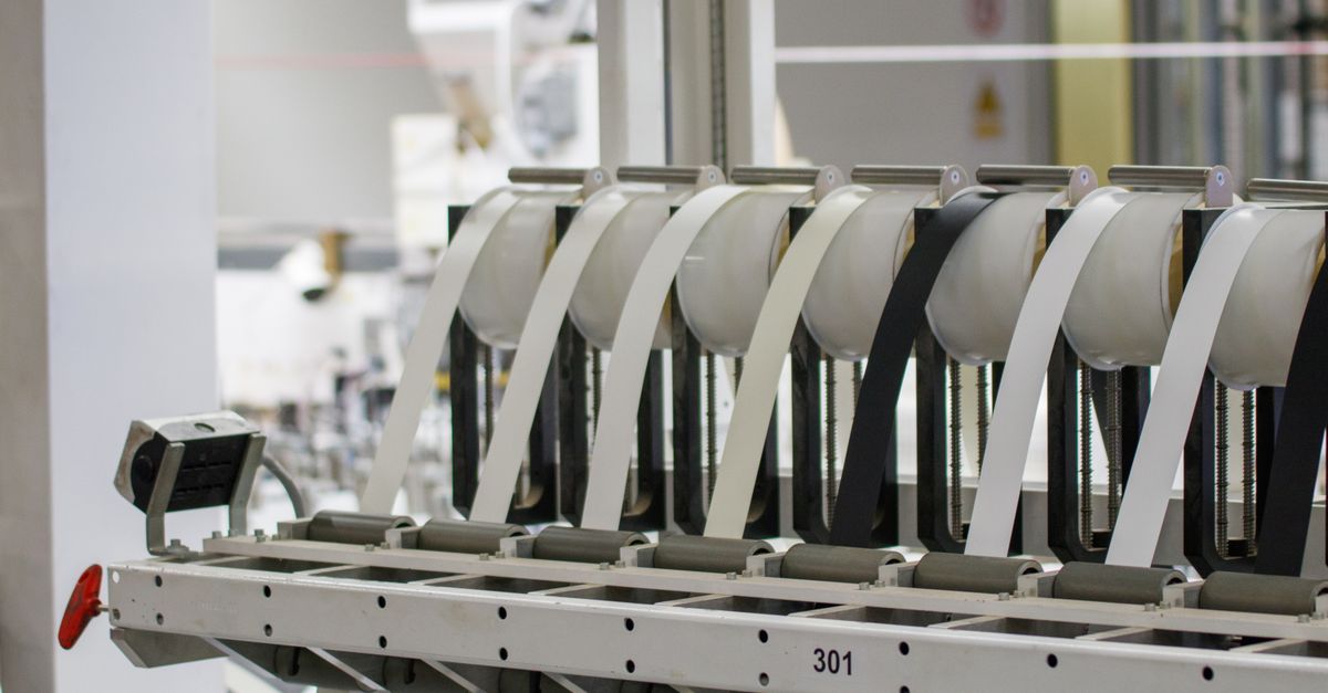
Deep learning approaches are transforming inspection capabilities that traditional rule-based systems cannot match. Current state-of-the-art optical and electron beam inspection systems rely on rule-based techniques for defect detection and classification, which are usually rigid in their comparative processes, limiting overall capability and increasing relative engineering time to classify nuisance defects. Intelligent inspection systems built on computer vision and deep learning now process thousands of parts per minute, catching microscopic anomalies that human eyes cannot reliably detect.
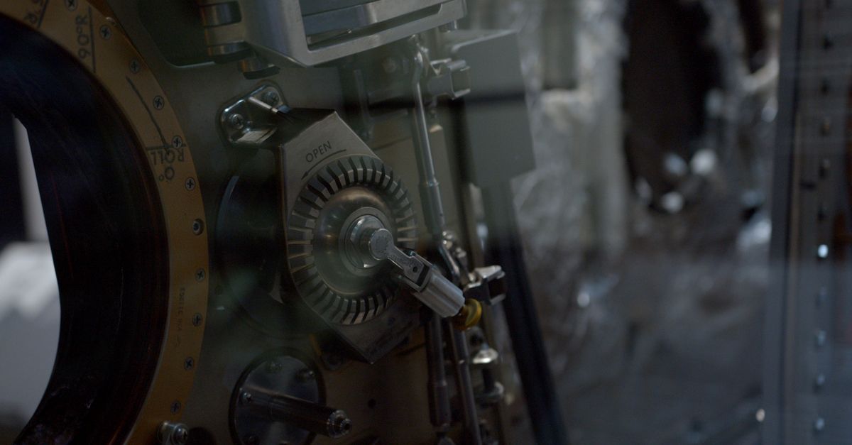
Hybrid bonding processes present unique challenges for defect inspection, particularly at wafer edges. Edge roll-off is the gradual thinning or height loss near the edge caused by processes such as grinding, chemical mechanical planarization (CMP), coating, and edge trimming, and hybrid bonding in advanced packaging means tighter overlay and thinner wafers, with wafer thinning increasing edge fragility. AI enables detection of previously invisible defects in these critical regions. Hybrid bonding requires tight process control, as any particle on the surface of wafers to be bonded can lead to void formation, and as critical dimensions and pitch for copper pads shrink, ever-smaller particles can lead to yield-killing voids.
Machine learning models are often combined with physics-based approaches rather than deployed in isolation. This hybrid approach provides superior robustness and enables extrapolation beyond training datasets. Deep learning, particularly convolutional neural networks (CNNs) and transformer-based vision models, can automatically classify defects with far greater accuracy and consistency, learning directly from labeled defect images and making them adaptable to new defect types without extensive manual reprogramming. Related advances in AI-driven analysis are improving manufacturing processes across multiple industries.
Why Do Chiplets Create Data Management Challenges?
The shift toward chiplet-based designs and advanced packaging architectures is generating unprecedented data volumes that stress existing analytics infrastructure. Multi-die packaging means each component requires inspection and metrology, multiplying the measurement burden. The demand for chiplet integration using 2.5D and 3D advanced packaging technologies has surged, driven by exponential growth in computing performance required by artificial intelligence and machine learning, with challenges related to bandwidth density, energy efficiency, electromigration, power integrity, and signal integrity.
Scalable analytics must handle both measurement density and production volume simultaneously. Millions of measurements per die across high-volume production create storage, processing, and correlation challenges that exceed the capabilities of traditional quality control systems. Chiplet integration requires high-density, high-bandwidth interconnects, which can be challenging to design and manufacture. Companies like PDF Solutions are developing specialized platforms to manage this data explosion, but infrastructure investment remains a barrier to scaling AI from pilot to production.
The move to more complex packaging also introduces new failure modes. Dies on the edge of the wafer may have different stress profiles than those at the center, and if die-level metrology isn’t performed, failures may be missed entirely. AI training on massive datasets can predict likely failure zones and adapt inspection patterns accordingly. Companies pursuing advanced hybrid bonding face particularly acute challenges managing defect data across multiple process steps.
What Separates Successful AI Deployments from Failed Pilots?
Organizations that successfully scale AI beyond pilots approach implementation differently from the outset. The 80-88% pilot failure rate reflects gaps in governance, infrastructure readiness, change management, and executive ownership — not model quality. Production environments lack the clean data, dedicated teams, and limited scope that characterize controlled pilots. An AI pilot is a controlled experiment with clean data, dedicated team, limited scope, and minimal integration requirements, while AI operationalization is a fundamentally different challenge.
The Google Cloud DORA 2025 report attributes 70% of AI transformation value to people, organizations, and processes, not to the technology itself, yet only 37% of organizations had invested significantly in change management, incentives, or training alongside AI deployments. Successful implementations require infrastructure built before pilots begin, not retrofitted afterward. Data quality, correlation capabilities, and robust connectivity between inspection tools become critical when scaling from single-line pilots to fab-wide deployment.
The semiconductor industry’s experience with AI scaling challenges parallels broader manufacturing trends. The companies that will win with AI are not the ones with the most advanced models, but the ones that approach implementation with rigor, patience, and a focus on measurable outcomes, and the 70 percent failure rate is not inevitable. Organizations must address organizational gaps—missing data infrastructure, absent governance frameworks, and metrics disconnected from business outcomes—before expecting pilots to scale successfully. Companies implementing AI across manufacturing operations face similar scaling challenges regardless of application domain.
Plant managers evaluating AI defect inspection systems should assess not just model accuracy but organizational readiness for scale. Before launching pilots, verify that data infrastructure can handle production volumes, establish governance frameworks, and secure executive commitment beyond the demo phase. Target high-value use cases like wafer edge inspection for hybrid bonding where AI capabilities clearly exceed traditional methods, but budget 60% of resources for change management and integration rather than software alone. The difference between a successful pilot and failed deployment often lies in infrastructure decisions made before the first model trains.
Q: Why do AI defect inspection models fail to scale despite successful pilot results?
Pilots operate in controlled environments with clean data and dedicated teams, while production requires integration with existing systems, governance frameworks, and real-time processing of massive data volumes from chiplet packaging. Most failures stem from organizational gaps—missing data infrastructure, absent change management, and evaporating executive sponsorship—rather than technical model limitations.
Q: How does hybrid bonding increase the need for AI-based wafer edge inspection?
Hybrid bonding requires tighter overlay tolerances and uses thinner wafers that are more fragile at edges, where edge roll-off and particles can cause yield-killing voids. Traditional inspection methods depend on repetitive patterns and struggle with partial die regions, while deep learning models can generalize across incomplete structures to detect previously invisible defects in these critical areas.
Article Source: AI Models Transform Defect Inspection And Review, But Can Fail To Scale