- Millions of defects now detected per wafer at advanced process nodes, overwhelming inspection systems.
- AI and machine learning at the edge can classify critical defects versus harmless nuisance errors.
- Advanced illumination modes capture multiple image types to identify true manufacturing problems.
- Edge computing reduces data bottlenecks by processing defect data at the inspection point.
Semiconductor manufacturers are grappling with an explosion of detected defects as process nodes shrink, with millions of potential issues flagged on each wafer. Onto Innovation is addressing this challenge by deploying AI and machine learning at the edge to separate critical defects from harmless nuisance errors caused by process variation. This shift to edge-based defect classification promises to streamline quality control workflows and prevent production bottlenecks for chip manufacturers.
The semiconductor industry faces a critical problem: as transistor geometries shrink below 7nm, inspection systems detect exponentially more potential defects, yet only a small percentage actually impact chip functionality. Traditional centralized analysis systems cannot keep pace with the data volumes generated by modern wafer inspection tools, creating delays that slow production and increase costs for fabrication facilities.
Why Are Defect Detection Rates Exploding at Advanced Nodes?
As semiconductor manufacturing pushes toward 3nm and 2nm process nodes, the sheer density of transistors and interconnects creates unprecedented challenges for defect detection. At these advanced nodes, inspection tools can identify millions of potential defects on a single wafer, driven by increased sensitivity required to catch smaller anomalies. However, the vast majority of these detected defects are what the industry calls “nuisance defects”—variations that appear anomalous to inspection systems but have no impact on chip performance or yield.
The problem stems from multiple factors. Process variation becomes more significant at smaller geometries, creating patterns that inspection algorithms may flag as defects. Neighborhood noise, where legitimate features in surrounding areas create false positives, also increases. Additionally, modern inspection systems use multiple illumination modes—brightfield, darkfield, and various angles—to capture different types of defects, multiplying the data generated per wafer. Each illumination mode reveals different aspects of surface features, generating distinct images that must all be analyzed and correlated.
This creates a data management crisis. Centralized systems that process all defect data at a remote server or data center face bandwidth constraints and latency issues. By the time defect data is transmitted, processed, and classified, valuable production time is lost. For high-volume manufacturing facilities producing thousands of wafers monthly, these delays compound into significant throughput bottlenecks.
How Does Edge-Based AI Classification Solve This Problem?
Edge computing brings the intelligence directly to the inspection tool, processing and classifying defect data where it’s generated. Rather than transmitting millions of defect images to a central server, AI models deployed at the edge can immediately analyze each detected anomaly and classify it as either a critical defect requiring attention or a nuisance defect that can be filtered out. This approach dramatically reduces the volume of data that needs to be transmitted and stored, while accelerating decision-making.
Machine learning models trained on historical defect data can recognize patterns that distinguish real problems from harmless variations. These models learn to identify defect signatures across different illumination modes and inspection touchpoints, understanding which combinations of features indicate actual yield-limiting defects versus process noise. The models continuously improve as they process more wafers, refining their classification accuracy over time.
The edge deployment offers several technical advantages. Latency drops from minutes or hours to seconds, enabling real-time feedback to process engineers. Network bandwidth requirements decrease by orders of magnitude since only classified critical defects need to be transmitted for human review. Storage costs also decline as nuisance defects can be filtered out immediately rather than archived. For semiconductor fabs operating on razor-thin margins, these efficiency gains translate directly to improved profitability and faster time-to-market for new chip designs.
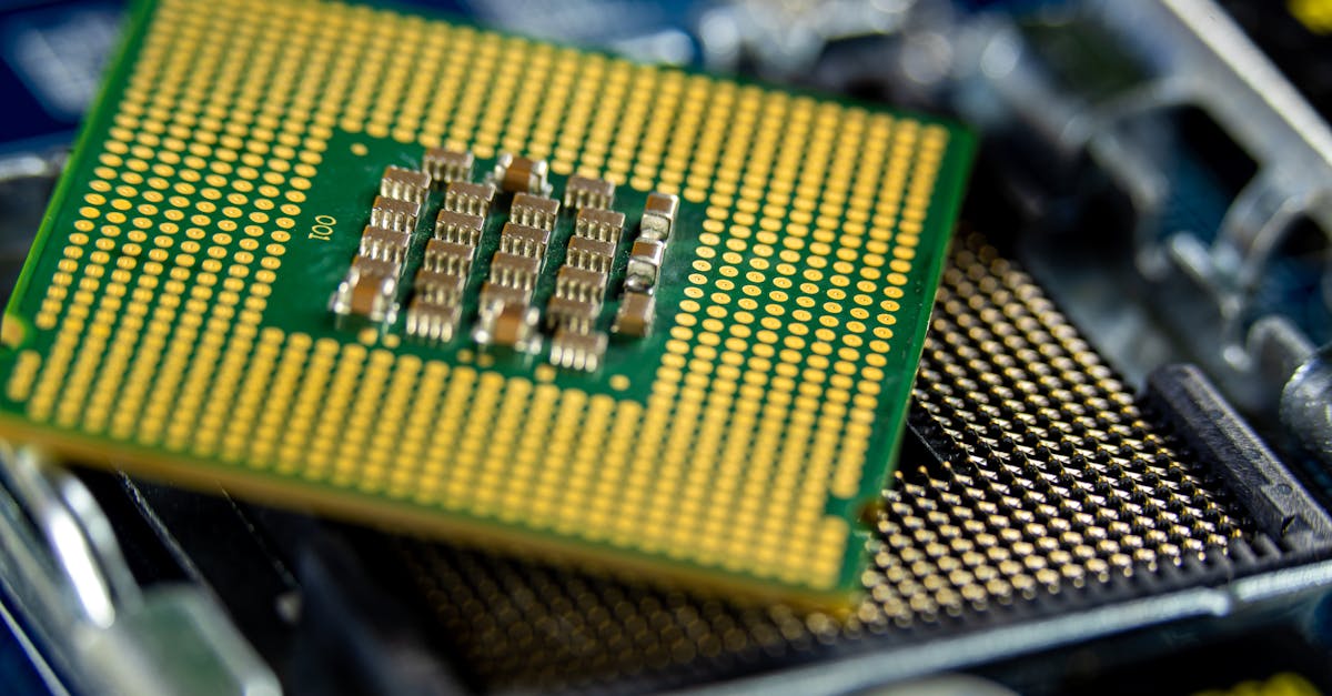
The implementation requires specialized hardware capable of running inference models at the inspection tool itself. Modern AI accelerators and GPUs designed for edge deployment provide the computational power needed to process high-resolution defect images in real time. The software stack includes trained neural networks optimized for defect classification, integrated with the inspection tool’s control systems to enable automated decision-making.
What Are the Broader Industry Implications?
The shift to edge-based defect classification represents a broader trend in advanced manufacturing toward distributed intelligence. Rather than centralizing all data processing and decision-making, Industry 4.0 principles emphasize placing computational capabilities where they deliver the most value. For semiconductor manufacturing, this means embedding AI directly into inspection, metrology, and process control equipment.
This approach aligns with the semiconductor industry’s push toward autonomous manufacturing, where smart systems make real-time adjustments without human intervention. As fabs implement more sophisticated process control strategies, the ability to instantly identify and respond to critical defects becomes essential. Edge-based AI enables closed-loop control systems that can detect problems, classify their severity, and trigger corrective actions within minutes rather than hours.
The technology also addresses growing concerns about data security and intellectual property protection. Transmitting detailed defect images across networks creates potential vulnerabilities, as these images contain proprietary information about manufacturing processes and chip designs. Processing data at the edge minimizes data movement, reducing exposure to potential security breaches. Only aggregated results and critical defects need to leave the inspection tool, limiting the information available to potential adversaries.
Beyond semiconductors, this edge-based defect detection paradigm is applicable to other precision manufacturing sectors. Aerospace component inspection, automotive electronics production, and medical device manufacturing all face similar challenges with high-resolution inspection generating massive data volumes. The techniques developed for semiconductor defect classification can be adapted to these industries, spreading the benefits of edge AI across advanced manufacturing.
Key Takeaway: For plant managers and process engineers in semiconductor manufacturing, the transition to edge-based AI defect classification offers a clear path to managing the data explosion at advanced process nodes. By investing in inspection systems with integrated AI capabilities, fabs can maintain production throughput while improving defect detection accuracy. The key is selecting systems with robust machine learning models that can be trained on facility-specific defect libraries, ensuring the AI understands the unique signatures of your manufacturing process. As nodes continue to shrink toward 2nm and beyond, edge intelligence will transition from competitive advantage to operational necessity.
Frequently Asked Questions
Q: What types of defects are considered “critical” versus “nuisance” in semiconductor manufacturing?
Critical defects are anomalies that will cause chip failure or yield loss, such as particle contamination bridging conductors, missing metal lines, or severe pattern distortions. Nuisance defects are variations flagged by inspection tools that don’t impact functionality, including minor edge roughness, process-related texture variations, or false positives from optical artifacts. The classification depends on defect size, location, and the specific process layer being inspected.
Q: How much training data is required to develop effective edge AI defect classification models?
Effective models typically require thousands to tens of thousands of labeled defect images representing the full range of critical and nuisance defects for a specific process. The exact amount depends on defect complexity and process variation, but transfer learning from pre-trained models can reduce requirements. Models improve continuously as they process production wafers, refining classification accuracy over weeks and months of operation.
Q: Can edge-based defect classification systems integrate with existing fab control systems?
Yes, modern edge AI inspection systems are designed with standard interfaces compatible with fab execution systems, statistical process control software, and yield management platforms. They typically communicate through industry-standard protocols like SECS/GEM, allowing defect classification results to feed directly into existing quality control workflows. Integration complexity varies depending on legacy system architectures, but vendors generally provide middleware to bridge older systems.
Article Source: Moving Defect Detection And Classification To The Edge